
| Table of Contents | |
|---|---|
| Introduction | - Object of this article. |
| Modulation Modes | - Basic info about modulation. |
| Classes of Bias | - Basic info about classes of bias. |
| Class-A Amplifier | - One transistor amplifier project. |
| Class-AB Amplifier | - Two transistor amplifier project. |
| Component Values | - Rough/easy guide to component selection. |
| Transformers | - And how they are constructed. |
| Prototype Design | - A (belated) prototype for this project. |
| Conclusion | - A few parting words and tips. |
This is both a project AND a bit of basic theory regarding the design of wide-band HF power amplifiers. As usual, it is prompted as a result of e-mail in which I have to repeat myself over and over again. The object is to show a couple of basic configurations and practical examples of QRP linear amplifiers, although I have somewhat oversimplified a few things. But as an author I have the right to do this! So I will NOT delve deep into mathematics or give loads of formulas, but some degree of calculation is needed by the reader. I shall try to make it as simple as I possibly can, but you may need to take your socks off.
A "Linear Amplifier" is just an amplifier that does not create excessive distortion, and it can be used to amplify a ready-modulated signal without changing the characteristics of that modulated signal. It can be used for amplifying most transmission modes, for example:
| CW | Continuous Wave | - Unchanging frequency or amplitude, usually interpreted as Morse Code. |
|---|---|---|
| AM | Amplitude Modulation | - A CW signal, the amplitude of which conveys information. |
| DSB | Double Side-Band | - Amplitude Modulation with unused component removed. |
| SSB | Single Side-Band | - Amplitude Modulation with unused and duplicated components removed. |
| FM | Frequency Modulation | - A signal with constant amplitude but varying frequency. |
There many other modes, but I am only concerned with the above, which compromise the major modes I am interested in. CW and FM have an unchanging amplitude to convey information so non-linear amplifers are not really required, but it does no harm to use a linear amplifier to amplify CW and FM signals. Linear Amplifiers may be quite frequency conscious, making them unsuitable for such techniques as "frequency Hopping" or even video. In this article I will be concerned with wideband (untuned) amplifiers for use in the HF band (1MHz to 45MHz).
Another use of the "power Amplifier", is for use in receiving antenna distribution systems. You may wish, for example, to use one antenna for a whole housefull of receivers. The linear power amplifier is an excellent unit for this purpose, between the antenna and the passive signal splitter. Yet another, further, different use is that of amplifying antenna signals where there is the likelyhood of strong "in-band" or close signals could "block" a normal low-power receiver pre-amplifier.
Before we continue, perhaps a word about "Classes of Bias". The info I give here is perhaps a little over simplified, so the more experienced reader may wish to jump over this section. The next section (Class-A project) is coloured dark green.
When a signal is applied to a transistor, that signal comprises both positive and negative swings of current or voltage. Unfortunately, transistors cannot handle a negative current, so we must add a standing bias current. To this current will be added and subtracted signal currents, so this bias must exceed the maximum signal in the negative 1/2 of the signal waveform. This is Class-A bias. It is used in single-transistor amplifiers but has a poor efficiency, practically not greater than 45%.
Class-B dictates the device has little or no standing DC current and therefore amplifies positive 1/2 waves of the applied signal. Due to the lack of a standing and heavy DC current, it is a lot more efficient than class A. When applied to a single device it creates a LOT of distortion, but when used in a complementary or push-pull amplifying configuration, little distortion will result. A practical efficiency would be in the order of 80%.
This class of amplification is where the device is biassed somewhere between class-A and Class-B and when used in a complementary or push-pull amplifying configuration, little or no (comparatively) distortion will result.
There is another class of amplification: Class-C. I will mention this in passing but I will not be concerned with this class in this article. Class-C is where the amplifying device is heavily cut-off (non-conducting) so that small signals are not even amplified at all. This generates tremendous distortion and harmonics, both odd and even. This class of amplification can only be used for ultra-efficient amplifiers without any amplitude information, such as CW and FM. It is useless for AM and SSB. Because of all the harmonics, Class-C is used in frequency multipliers.

This is a typical single-transistor Class-A amplifier. R1 and R2 divide the supply voltage to feed the Base of the transistor, via the secondary of T1. This normally sets the Base to about 25% of the supply voltage. R3 emitter resistor sets the standing DC current through the transistor. T2 matches the collector to the load.
The single transistor circuit is quite capable of delivering several watts of RF power, with the correct choice of components. The big disadvantage of this circuit is that TR1 must have a high standing DC current, which usually means the transistor must be fitted with a heat-sink. Another downfall is that the "hfe" of transistors fall with increased current. This means that as the RF signal changes it's level throughout the cycle, so, too, will the gain of TR1. As the current rises, the gain falls. The following diagram shows quite clearly the effect on the RF output signal.

Waveform #1 is the desired waveform but if the transistor is not grossly under-rated then waveform #2 is what you will get. As you can see, this introduces a LOT of 3rd harmonic. It may not be as bad as shown, yours may 20dB or 30dB down so it will look perfect to the naked eye. Your neighbours may have other views, especially if they are trying to watch "The Bold & The Beautiful" on their one-eyed god. If you over-rate the transistor (use a 10 watt transistor to drive only 1-watt) and use a decent output low-pass filter, then all should be well.

Here is a better solution. TR1 and TR2 each amplify opposite halves of the RF wave-form and each half is combined in T2, which matches TR1 and TR2 to the load. Again, R1 and R2 divide the supply voltage to feed the Base of the transistors, via the secondary of T1. This is normally set to about 1-volt so TR1 and TR2 are conducting just a small amount of current. If a trough in the waveform causes a transistor to stop conducting then there is no problem, the other transistor will be doing the work. The emitter resistor limits the current and improves linearity.
Since this amplifier is symetrical, the third harmonic will be greatly reduced, as long as at least one of the transistors is always conducting something. So in effect, one transistor amplifies the +ve 1/2 cycles and the other transistor amplifies the -ve half cycle.

Waveform #3 represents a decent sinewave for comparison, but waveform #4 shows you what happens if the class of bias changes from Class-AB to Class-B and beyond. This particular circuit is efficient, typically 80%, and only dissipates any significant heat during RF activity. This circuit can be used to deliver RF power from 100mW to well over 100-Watts, with suitable choice of components.
The Class-A amplifier must be so biased as to have a standing current exceeding the maximum signal current variations. So let us begin at the output, since it is the output power that dictates the bias current. Let us assume we want a 100mW output power and the supply voltage is 12-volts (13.8v). The circuit we shall be using is:
With a 12 volt (13.8v) supply, the complete sine-wave peak-to-peak value can only vary from about 2-volts to about 13 volts, or a total swing of just over 10 volts. The RMS value of voltage is therefore 10 x 0.3535 = 3.5 volts. This is the maximum amplitude of our output voltage at the collector of TR1. To deliver 100mW of power, with only 3.5 volts, we need a current of W / E = I or 0.1 / 3.5 = 0.028 Amperes = 28mA. Since this is the RMS value, then the peak current will be 28 x 1.414 = 40mA. So the output signal at the collector of TR1 needs to vary from -40mA to +40mA at peaks. We must therefore add a standing bias that is greater than 40mA, say, 50mA. So now the current will vary from 10mA to 90mA with an average value of 50mA.
I will select a transistor, such as the BC547, with an "hfe" of about 200. With 50mA standing Collector current, then the Base current is Ic / hfe = 50mA / 200 = 0.25mA. This means that R1 + R2 must burn at least 2.5mA (10 x Base current), so R1 + R2 must be about 5520 Ohms. R1 = 4K7 and R2 = 820R would be a good division using preferred resistor values, and this would give about 2.05 volts at the Base of TR1, resulting in 1.3 volts at the Emitter of TR1. R3 = Ve / Ie = 1.3v / 50mA = 26 Ohms. 27 Ohms would be close enough since I have rounded up the odd number here and there.
C1 and C2 should just be big-ish. 22nf would be fine and the electrolytic is normal practice for RF. 47uf is fine. C3 will increase the gain, but also increase distortion quite a lot.
The Class-AB amplifier does not need be so biased as to have a standing current exceeding the maximum signal current variations. Just a small standing current of 5mA is adequate for up to about 1 Watt, 20mA for up to 10 watts and 80mA up to 100 Watts. But we will make an amplifier for 5 Watts using 2SC2078, a device used for CB RF output transistors. You can pick other devices, such as 2SC3781 - a line-output transistor for portable TV sets. Let us assume we want a 5 Watts output power, and the supply voltage is 12-volts (13.8v). The circuit we shall be using is:
Since two devices are each handling 1/2 the input waveform then the peak collector voltage of one device will be about 12v volts and the RMS collector-to-collector voltage will be about 8 volts. To deliver 5 watts, the RMS current will be W / E = I or 5 / 8 = 0.625 Amperes = 625mA. Since this is the RMS value, then the peak current will be 625 x 1.414 = 885mA. Each transistor will therefore be conducting almost 1 Ampere at signal peaks. Using a power transistor with Hfe = 80 then Base current is going to be about 11mA. R1 + R2 = 13.8v / 11mA = 1254 Ohms. This time I will increase the current a little and use resistors of R1 = 1K0 and R2 = 100R. This means the emitters of the TR1 and TR2 will be about 0.5v DC. R3 should drop no more than 1 volt at full output (900mA) so 1 Ohm will be about right here, BUT the 100-Ohm resistor must be reduced in value to set the standing bias current to 10mA or so. R2 should therefore be a preset variable resistor.

Another variation that would be more stable would be to replace R2 with an ordinary silicon diode. R1 could therefore be selected to give TR1+TR2 standing current of 10mA and no adjustments need be made, even with varying supply voltages.
As a general "rule of thumb" you can assume the input impedance of a stage is equal to the emitter resistor. It may not be 100% accurate, but it will put you in the right area and is certainly close enough for winding coils. In all these examples I used torroidal transformers. These comprise a ferrite slab with two holes through them. You can place two ferrite beads together and treat them exactly the same - this is what I do, and it is cheaper. This is the method I used in this photograph:

T1 is designed to match the input to the base of the transistor. In our 100mW Class-A single transistor amplifier, the base impedance is a little uner 25 Ohms, and the input is 75 Ohms. With an impedance ratio of (making the numbers easy) 80:20 = 4:1. The turns ratio is the square-root of the impedance ratio = 2:1. 8-turns primary and 4-turns secondary. I have always found it advisable to feed transistors a little lower impedance. The circuit then becomes more predictable, even with different transistors. I picked 8-turns for the 50/75-Ohm winding because experience has taught me that this is a good general figure that works from 1MHz to 40MHz with most ferrites.
T2 in the 100mW circuit matches the load to the collector of the transistor. When working out the collector impedance FORGET THE DC BIAS. It is only the signal that is of interest. In out 100mW amplifier we had 3.5vRMS at 28mA, so the collector impedance is 3.5/.028 = 125 Ohms. To match 125 Ohms to 75 we need an impedance ratio of 125:75 = 1.7:1 or a step-down turns ratio of 1.3:1. T2 could have two configurations - 8 turns with a tapping at 2 turns from the collector - OR - 8-turns primary with 6-turns secondary.
The 5-watt version has a much lower Base impedance. In this case it is around 1 Ohm for each transistor. If the input is 50/75 Ohms then the impedance ratio is about 64:1+1 which is a nice round figure of 8:1+1 turns ratio. 8-turns primary winding and 1+1 turns secondary. This means 2-turns with a centre-tap. Use a little thicker wire for the lower impedance windings.
The 5-Watt version output transformer must match 8 volts (RMS) at 625mA = 12.5 Ohms to the output of 50/75 Ohms. Interesting that for 50-Ohms the impedance ratio is 1:4 so the turns ratio is 1:2 (2:4). The primary is tapped, so 1+1:4 is the correct turns ratio. The primary consists of 4-turns with a centre-tap (2-turns + 2-turns) and the secondary of 8-turns.
You could make a multi-stage transformer in exactly the same way - assume somewhere around 8-turns to 12-turns is 50/75-Ohms and wind accordingly. If you had, for example, the 100mW version feeding the 5-Watt version to make a 3-transistor Power Amplifier, then the coupling transformer will be "T2 100mW Primary" and "T1 5-Watt Secondary". This would be 4 + 4 primary and 1 + 1 turns secondary, just like this:

When I look in my junk-box I find many ferrites. I pick the GREY ones for RF use. The miniature ferrites I use are about 3mm Diameter with a 1mm hole. The length is about 4mm. These ferrites work well up to about 1 watt of power. One of the most common mistakes is to use ferrites that are too big. The larger they are then the worse they are at higher frequencies. The ferrites I use here seem to work well up to 150MHz without a problem. You do, however, need bigger ferrites above about 1 watt. Today they are expensive or hard to get but I have had some success modifying "junk-box-ferrite". If you want to drill ferrites then freeze them in a large block of ice and use nice new tungsten drill bits in a high-speed drill.
This is the difficult bit. I have already used these circuits as building-blocks for many years, so it is a bit late to start talking about prototypes. So I propose to just "throw together" a prototype 250mW QRP linear amplifier, using Class-AB and include the mandatory low-pass filter on the PCB. The board has sufficient space to add larger ferrites and the transistor pin-spacing allows you to insert TO220 power devices to make that larger 5 Watt amplifier. The TO220's may be mounted below the board, bent over and bolted to a heatsink. This will also support the PCB, but it is a bit fiddly when it comes to positioning the legs and bending them over. You even could modify the artwork a little to use two pairs of BC547 transistors and get 600mW out (T2 secondary = 5 turns).
But I will continue with my 2x BC547 and be content with 250mW. I don't normally give PCB component layouts here due to limited space on the projects server, but in this case I will make an exception since it is only 12K. Here is the simple amplifier. It only needs 5mW of drive at 1.8MHz to give 300mW out so it makes an ideal addition to an AM oscillator to generate AM or QRP SSB signals.
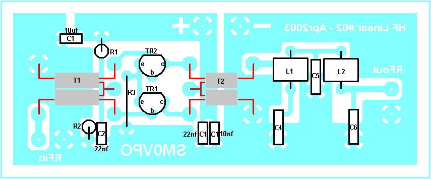
The circuit to accompany this PCB is:

As you can see, the circuit is exactly as discussed above: yet another case of simple is good. Component values would be:
R1 = 4K7, R2 = 1K0, R3 = 47R, C1 = 10n + 22n + 10uf, C2 = 22nf,
T1 = 8-turns
primary plus 4-turns secondary with centre-tap,
T2 = 8-turns primary with centre-tap
plus 4-turns secondary.
| Frequency Dependent Components | |||||||
|---|---|---|---|---|---|---|---|
| 1.8MHz | 3.5MHz | 7MHz | 10MHz | 14MHz | 21MHz | 28MHz | |
| C4 | 1800pf | 1000pf | 470pf | 350pf | 150pf | 100pf | 91pf |
| C5 | 2700pf | 1800pf | 820pf | 610pf | 330pf | 220pf | 180pf |
| C6 | 1800pf | 1000pf | 470pf | 350pf | 150pf | 100pf | 91pf |
| L1 | 4.80uH | 2.75uH | 1.40uH | 1.05uH | 0.70uH | 0.46uH | 0.35uH |
| L2 | 4.80uH | 2.75uH | 1.40uH | 1.05uH | 0.70uH | 0.46uH | 0.35uH |
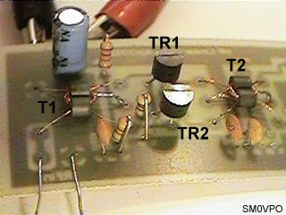
When it is all built it looks something like the photograph below. Here you can see the coil construction quite clearly and that there is loads of space for much larger ferrites than the little tiddley ones I have chosen. The rest of the board is quite well spaced out so there is plenty of room for using larger components than those I chose. This particular photograph, however, is is the same board foil I have provided but the push-pull output also drives another push-pull output stage to give 5 watts out.
I have avoided mathematics as much as possible and tried to use simple Ohm's Law and "finger maths" with a description. For example the output collector impedance of an amplifying stage is given by the expression "Vcc squared over output power in Watts". This, however, is a MAXIMUM value. The impedance may be a little lower, but never higher. In this respect I believe that a little explanation and finger-maths is more than adequate for the amateur constructor. If you wish to go deeper then do as I did - buy books and read.
If you now want to see an older project based upon the information given on this page then look at my 10 Watt Power Amplifier project Since this project will deliver over 15 Watts a little more attention has been paid to neutralising (330R + 10nf) and bias control. The bias control is even temperature compensated.
So now all you have to do is to wait until I can add the PCB foil pattern file to my download section and you can start building your own QRP transmitters based on my design. Small tip for you, a 5-turn loop around the coil of my Grid Dip Oscillator (GDO) will provide several milliwatts of RF drive - an excellent testing tool.